
Wafer annealing has become a key step during semiconductor manufacturing, allowing us to enhance the properties of an SI wafer. Under very specific circumstances, by heating and then cooling a wafer, we can improve the silicon’s crystallinity, activate dopants, and relieve stress within the material.
Depending on the materials used, the wafer’s future applications, and the manufacturer, several proven methods for wafer annealing exist. To help you understand how each one can optimize a semiconductor for the specific device performance and yield you’re looking for, we've created this breakdown.

There are various ways to classify wafer annealing, and each has special traits and uses:
The wafer is rapidly heated to high temperatures (usually between 600°C and 1200°C) briefly. RTA is perfect for activating dopants and creating shallow junctions because its quick heating and cooling cycles help reduce diffusion. This technique is frequently employed in MOSFET fabrication and ion implantation procedures.
Furnace annealing involves heating wafers in a controlled atmosphere within a furnace. In general, the temperatures fall between 600°C and 1000°C. This technique works well for procedures that need prolonged heat exposure, like low-temperature annealing, to relieve stress and oxide growth.
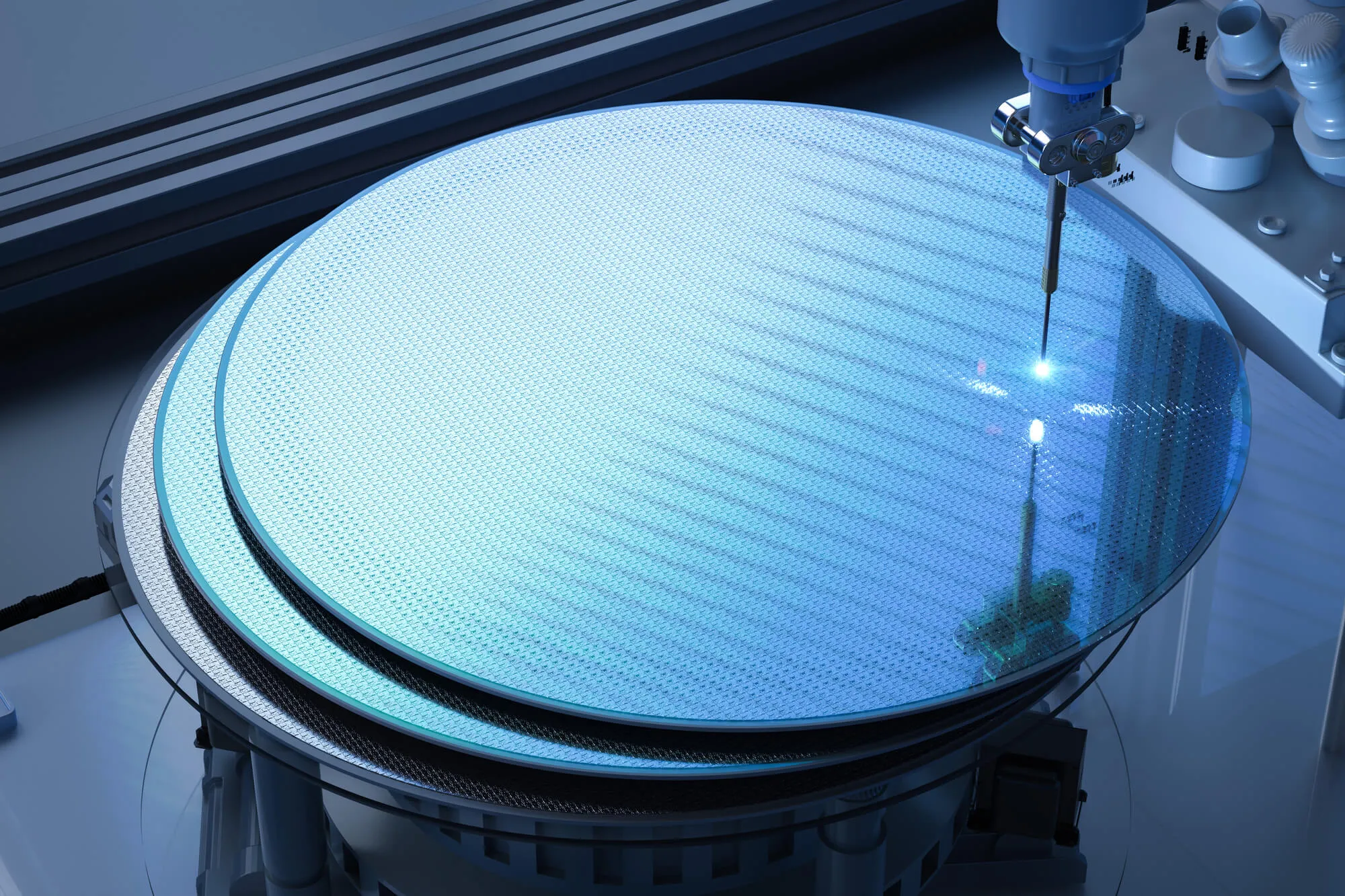
Focused laser beams are used in laser annealing to heat particular wafer regions quickly. This method allows specific areas of the wafer to be treated selectively without compromising the entire wafer, which is why it’s used for applications that need high spatial resolution.
This technique heats the wafer using microwave radiation. Rapid heating can be accomplished with microwave annealing while preserving a consistent temperature distribution throughout the wafer. This technique may benefit from materials with high thermal conductivity, like silicon carbide (SiC) and gallium nitride (GaN), which are frequently utilized in high-power and high-frequency applications.
Wafer annealing is an essential step in the fabrication of semiconductors. Depending on the needs and applications, it can be done in various ways. By knowing the benefits and drawbacks of each annealing method, engineers can improve yield and optimize device performance.
Here at Wafer World, we can help you determine the best annealing method for you. Contact us today for more information!


