.webp)
Stay up-to-date with the latest news and trends in wafer and semiconductor technologies.
*Blogs are for educational and informational purposes ONLY
See how silicon wafer suppliers help simplify wafer sourcing with clear specs, quality details, inventory planning, and project guidance.
Read More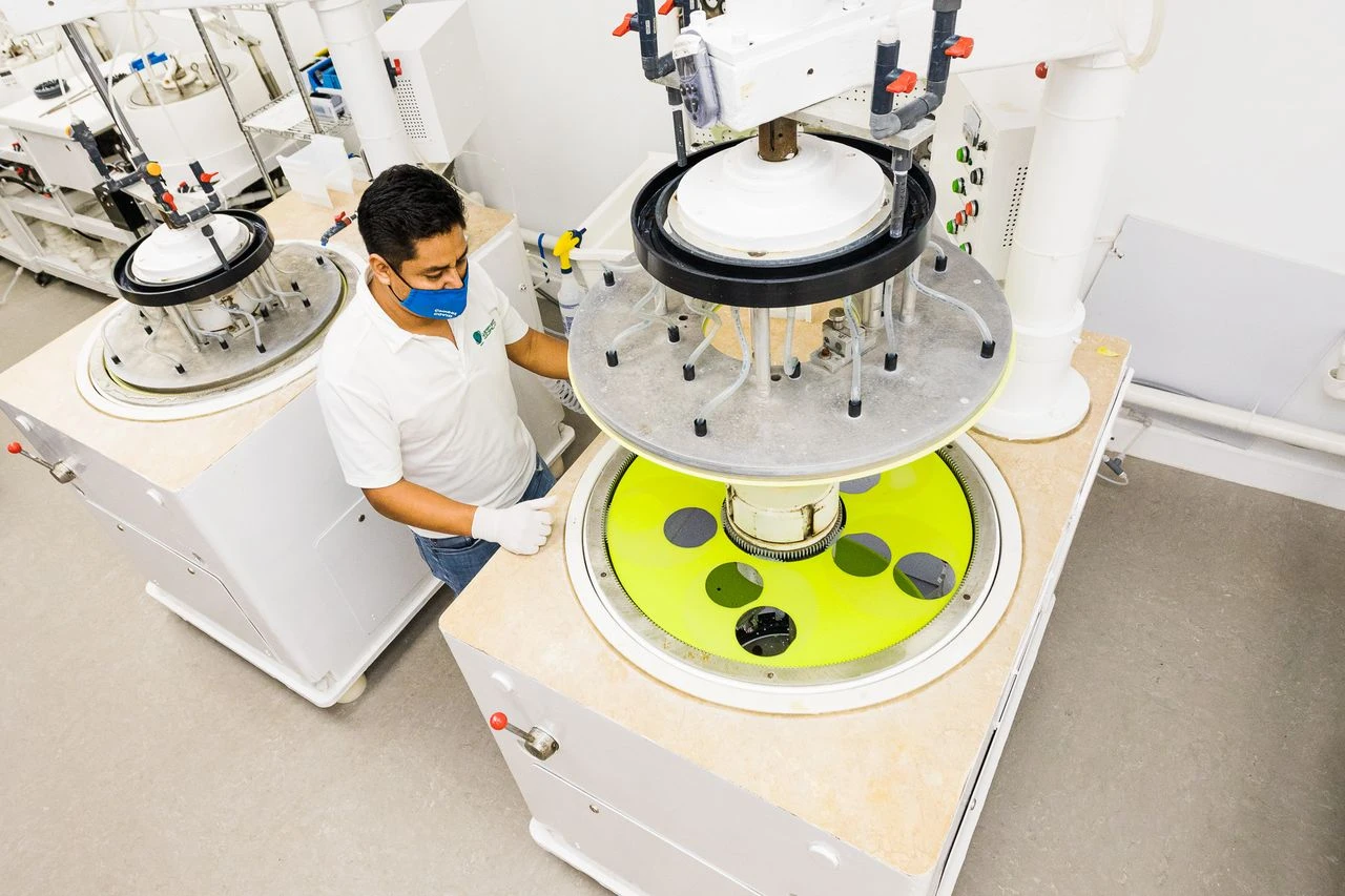
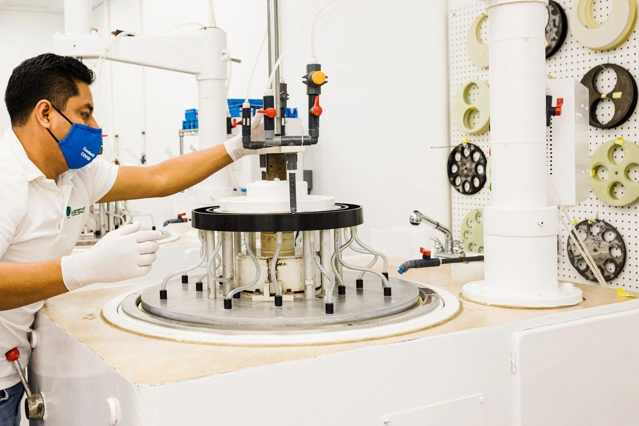
Explore how wafer manufacturing precision depends on equipment control, clean environments, testing, and consistent documentation.
Read More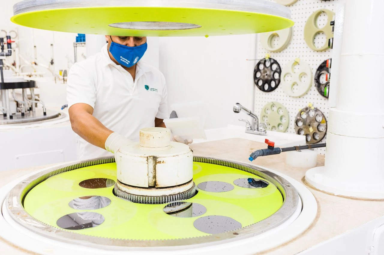
Compare silicon wafer suppliers by lead times, communication, inventory planning, and reliability before your next material purchase.
Read More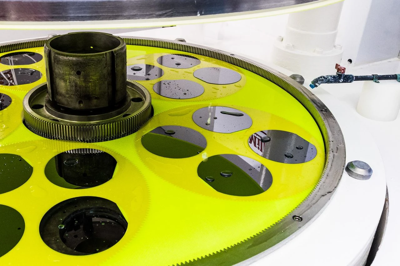
Compare R&D and production needs to choose the right silicon wafer specs, quality level, and buying approach for semiconductor projects now.
Read More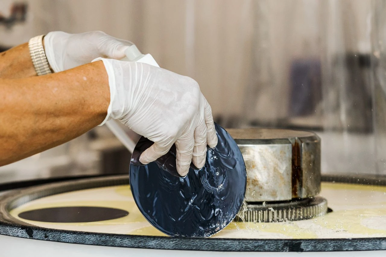
See how Si wafers are used in integrated circuits, sensors, research devices, & high-precision electronic systems.
Read More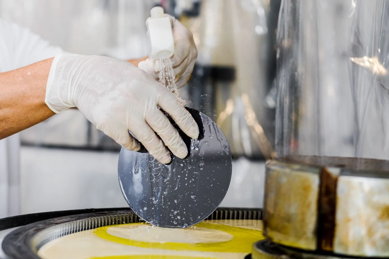
Here’s why flat zone wafer purity matters for advanced electronics, power devices, sensors, & precision manufacturing processes.
Read More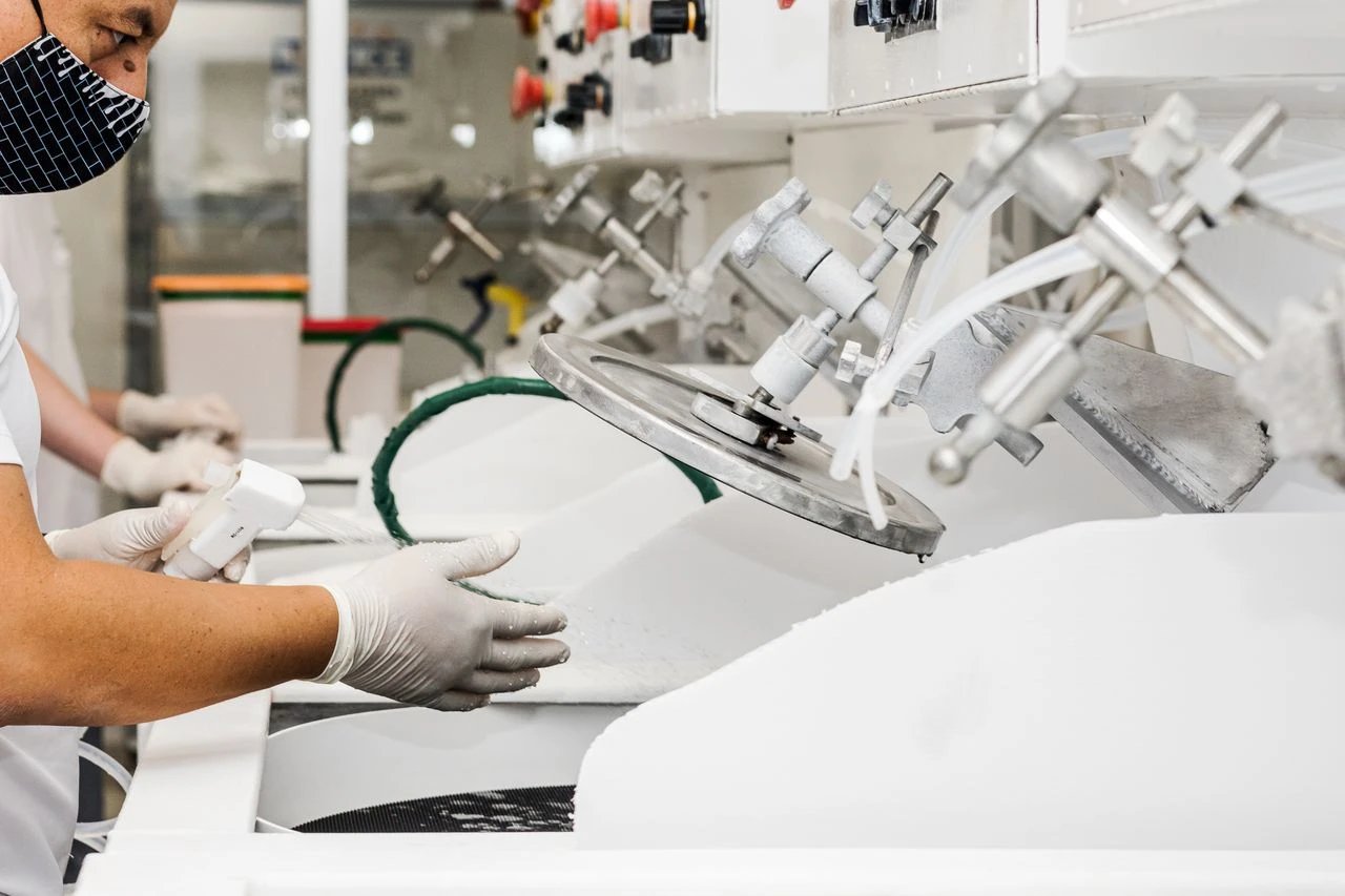
Here are the key stages involved in silicon manufacturing, including crystal formation, slicing, finishing, & defect control.
Read More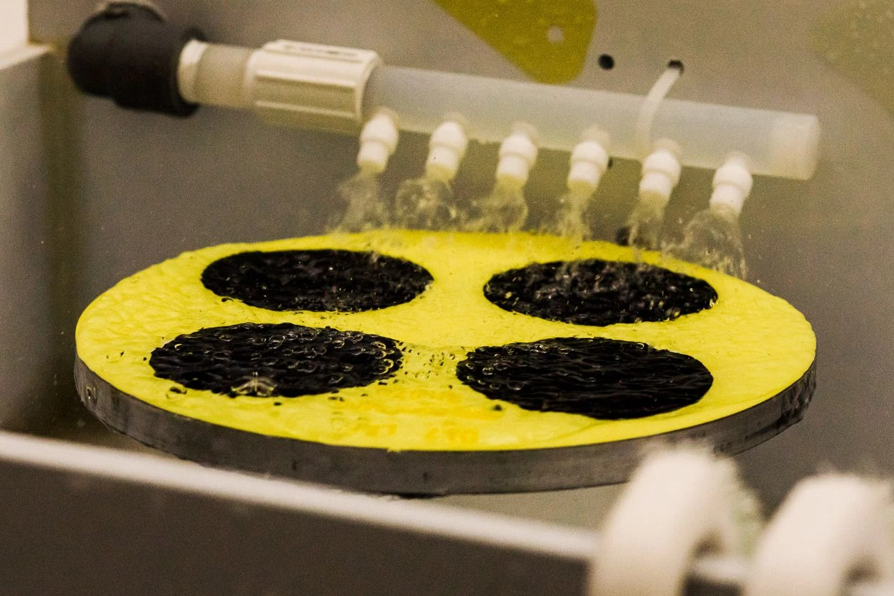
Learn how to buy silicon wafer products by reviewing wafer grades, crystal quality, thickness, resistivity, & surface standards.
Read More
GaAs reclaim wafers benefit from advanced surface restoration methods that improve wafer quality and usability.
Read More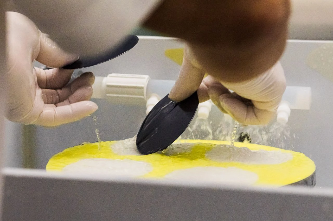
Learn how double side polish wafer processing improves surface quality, flatness, and semiconductor performance today.
Read More