"Wafer World has completed the acquisition of, MRT, Micro Reclaim Technologies as of January 1st 2026"
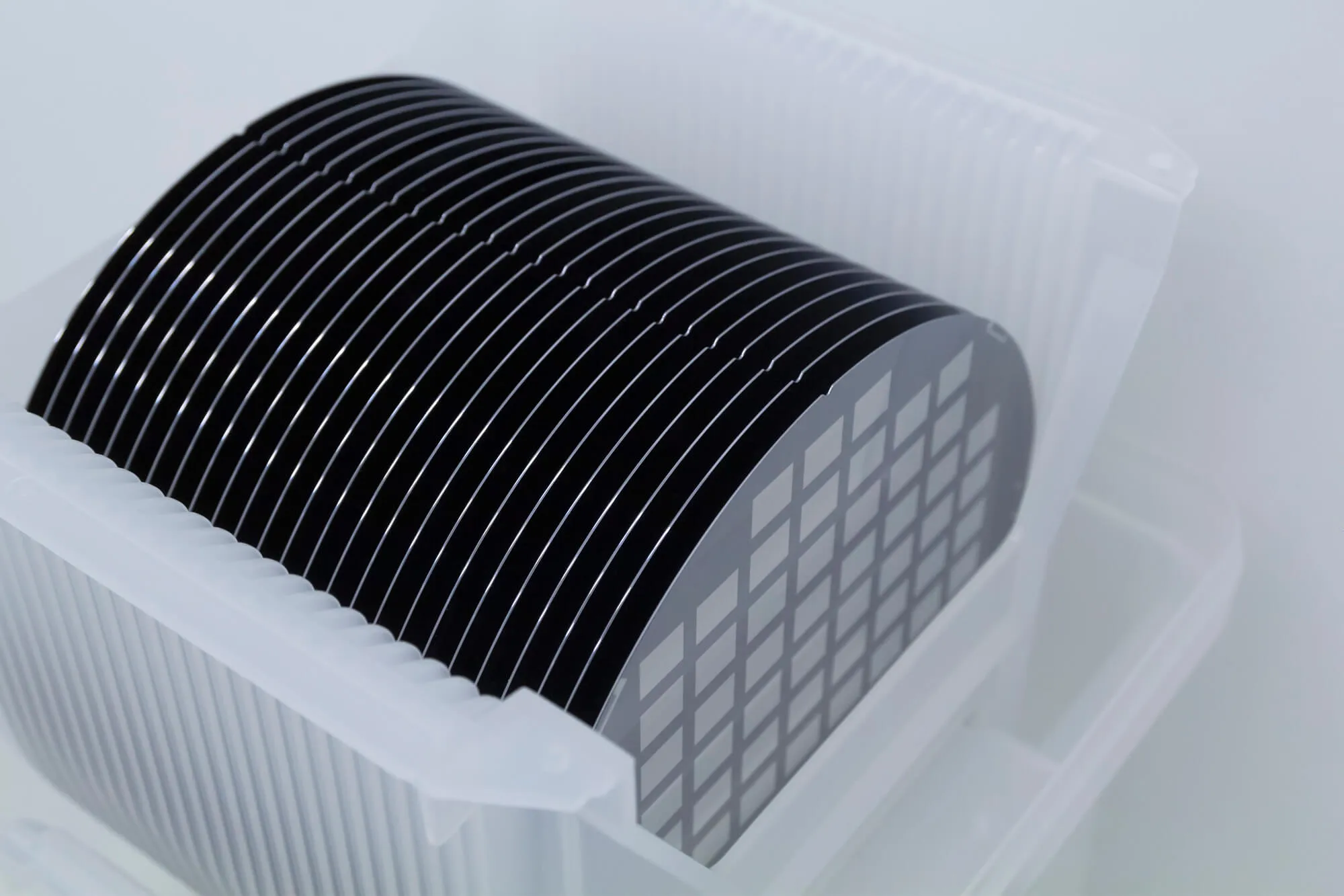
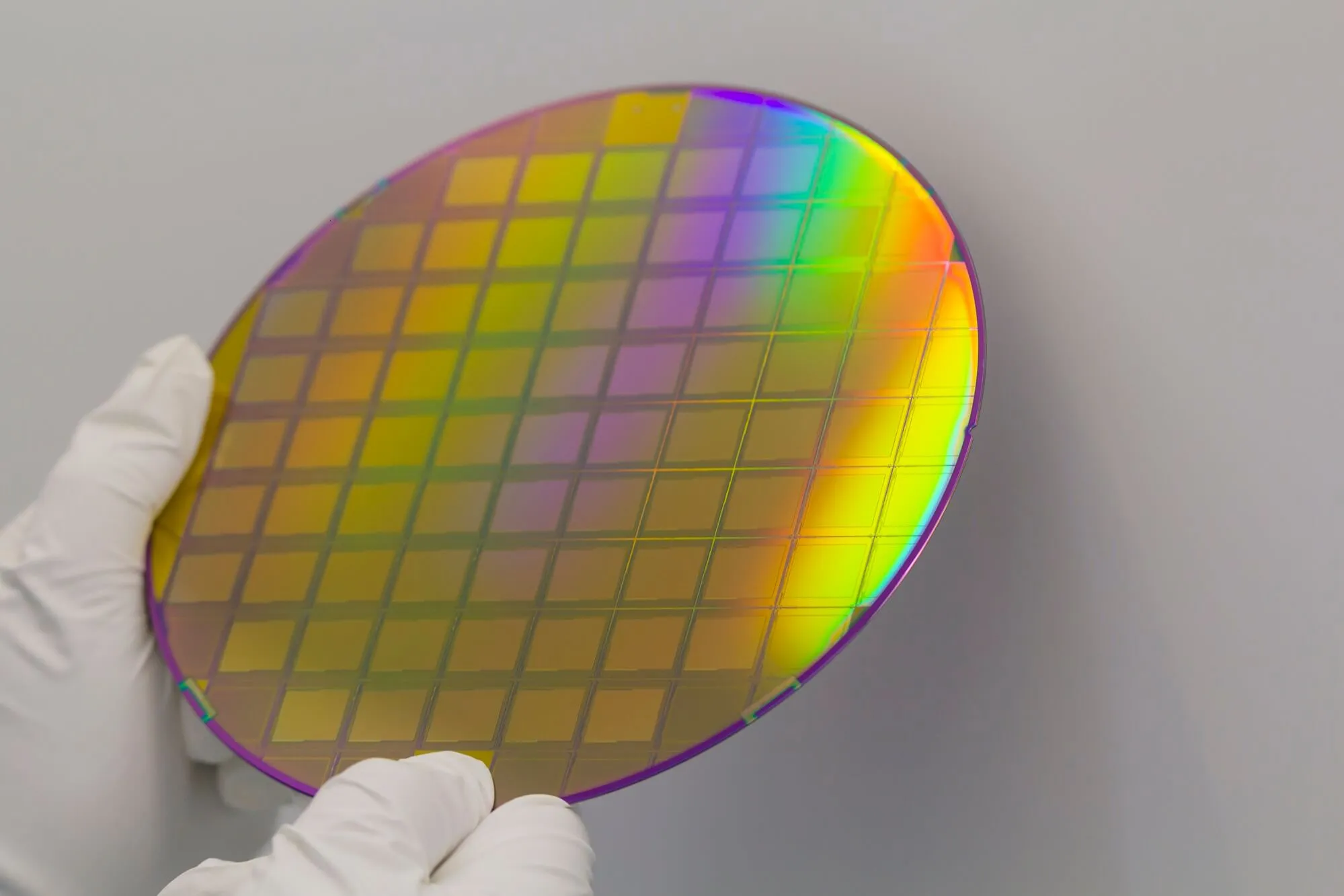
Float zone wafers, often referred to simply as "FZ wafers," play a crucial role in the world of semiconductor manufacturing. These wafers are known for their exceptional quality and purity, making them a preferred choice for various applications in electronics and photonics. However, if you're new to the world of FZ wafers, you probably have some questions. In this blog, we'll address some common FAQs about float zone wafers.

Float zone wafers are single-crystal silicon wafers grown using the float zone technique. This method involves melting a silicon rod and then solidifying it in a controlled manner to create a single crystal with high purity and minimal defects.
Float zone wafers are prized for their superior crystal quality and purity compared to other types of wafers. Their low defect density and exceptional electrical properties make them ideal for high-performance electronic and photonic devices.
FZ wafers are employed in various applications, including power electronics, high-frequency devices, solar cells, and sensors. Their superior material properties enable better performance in these fields.
Float zone wafer production involves a multi-step process that includes:
Yes, FZ wafers tend to be more expensive than other types due to the high-quality materials and meticulous manufacturing processes involved. However, their performance benefits often outweigh the cost.
Yes, float zone wafers can be recycled. Manufacturers often recycle wafers by reclaiming the silicon material and reusing it to produce new wafers, contributing to sustainability efforts.

Understanding float zone wafers and their significance in the semiconductor industry is essential for anyone working with advanced electronic and photonic technologies. If you have more questions or need specific information about FZ wafers, don't hesitate to reach out to Wafer World for guidance. Contact us today!