
Germanium has been a key material in the history of electronics and transistors, but its role was replaced by silicon so quickly that its valuable contributions have been severely overlooked. Today, a germanium wafer will find several uses, but it’s nowhere near competing with silicon in terms of mass usage.
However, studies are being made today to explore new ways in which germanium can replace—and outperform—silicon. Let’s help you understand the germanium wafer in perspective by covering the history of germanium wafers, explaining its current uses, and wondering about the possibilities that are to come.

EMBEB: https://youtu.be/8d7bW3SQY4w?si=K72oaH31QVGqlpO9
Around 70 years ago, two physicists from the Bell Telephone Laboratories, John Bardeen and Walter Brattain, pressed a slab of germanium with two thin gold contacts, and a third contact was made on the slab's bottom.
This allowed the current flowing through this arrangement to make a small signal larger. The outcome was the creation of the first transistor, regarded as the greatest invention of the 20th century. Transistors opened the door to the highly advanced computers we know today.
Despite its big role in the transistor’s early history, germanium was soon supplanted by silicon. Silicon is an abundant and much more affordable material. It has a wider bandgap, making it more difficult for current to leak across a device when it should be off.
Furthermore, silicon has higher thermal conductivity, which facilitates heat dissipation and prevents circuit overheating.
Despite silicon dominance in the semiconductor market today, germanium is still of deep importance in electronics.
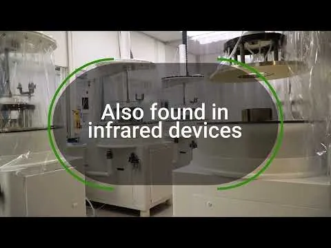
Several industries make use of germanium wafers. In the field of electronics, they are used in integrated circuits, diodes, and high-speed transistors, which perform better than silicon. Due to their ability to absorb infrared light, germanium wafers are also utilized in thermal imaging systems, night vision devices, and infrared optics.
Additionally, germanium wafers are significant in photovoltaics because they form the basis of highly efficient solar cells. They are also an essential component of fiber optics, which transmits signals over long distances. Moreover, this material may be poised for a comeback!
Many chipmakers are exploring alternatives to silicon as the core component of a transistor, the current-carrying channel. The idea is to replace the use of a material with a faster current flow rate that would allow engineers to create quicker circuits that utilize less energy. That way, better computers, mobile phones, and other gadgets that consume fewer resources could be developed.
In the beginning, III-V materials like gallium arsenide were the focus of all the excitement surrounding alternative channels. However, incorporating this material with current silicon technology is very costly, limiting the possibility of any GaAs technologies ever reaching the market of mass consumption. As a result, scientists began investigating the potential for a germanium-based transistor channel instead.
The first complementary metal oxide semiconductor (CMOS) circuits were made using germanium grown on regular silicon wafers. Additionally, a variety of transistor architectures, including nanowire devices, were built using the material.
Introducing germanium into the mixture is not as difficult as other materials. Moreover, chips that contain transistors that combine silicon and germanium in the channel have already been developed, like the transistors seen in a 2015 IBM and partner demonstration.
Moreover, germanium offers unique benefits. When these materials are near room temperature, germanium electrons move almost three times more quickly than in silicon. Additionally, holes—which are a material's electron voids that are handled like positive charges—move roughly four times as quickly.
Because germanium's electrons and holes are so mobile, it is a good material to use for CMOS circuit construction.
The faster these electrons and holes can move, the more quickly the subsequent circuits can move. Additionally, circuits can use much less energy because less voltage is needed to move those charge carriers.
For all of these reasons, germanium is an attractive option as a current-carrying channel. Performance can be greatly enhanced by the germanium channels, and the manufacturing difficulties should be easier to handle than with materials like GaAs.
However, there may also be certain shortcomings in the future regarding the adoption of this material.
There are still some rocks in the path of germanium that chip manufacturers need to sort before launching these transistors massively. Germanium or any other alternative channel material must be integrated into the dinner-plate-sized silicon wafers currently used to make chips in order to be produced in large quantities.
Fortunately, multiple attempts have been made to grow a moldable germanium layer into channels on a silicon wafer. Moreover, germanium's two main drawbacks—its higher cost compared to silicon and its relatively low heat conductivity—are greatly reduced when used in thin layers.
However, substituting a thin, superior layer of germanium in a transistor channel is not enough to replace silicon. The other components of the transistor and the channel must also operate perfectly.
Of course, germanium is not the only choice for transistor channels of the future. III-V materials, which can be used either alone or in combination with germanium, are still being studied. Moreover, a dizzying array of further possible developments in transistor technology, such as interconnection, are being developed.
This list includes channels made of a germanium and tin mixture, transistors operating via quantum tunneling, vertically oriented switches, three-dimensional circuits, and transistors made of carbon nanotubes.
In the upcoming years, we might end up implementing a few of these technologies.

Germanium wafers, though initially disregarded, have become an important semiconductor material because of their many applications and exceptional qualities. As technology develops, their significance is anticipated to increase even more, and several chipmakers are making efforts to address its shortcomings.
When that happens, early adoption is important to really foster revenue. If you’re interested in learning more about germanium wafers and their benefits, reach out to Wafer World!


