Semiconductor and silicon wafer suppliers are considered the ‘heart’ of electronic devices. Few people, nevertheless, are aware of the semiconductor raw materials that determine the shape of semiconductor chips.
Materials like silicon (Si), germanium (Ge), gallium arsenide (GaAs), phosphorus (P), boron, gallium, etc., can be used to create semiconductors for a wide range of appliances, from sophisticated rockets to smart, small devices like smartphones. In this article, we’ll discuss the raw materials of semiconductors and what benefits each has to offer.
In addition to the critical role that semiconductors play, raw materials play a big part in the semiconductor manufacturing process that powers the modern world of today.
Typical semiconductor raw materials consist of:
In the process of making chips, silicon—the main semiconductor raw material used in wafer fabrication—is essential.
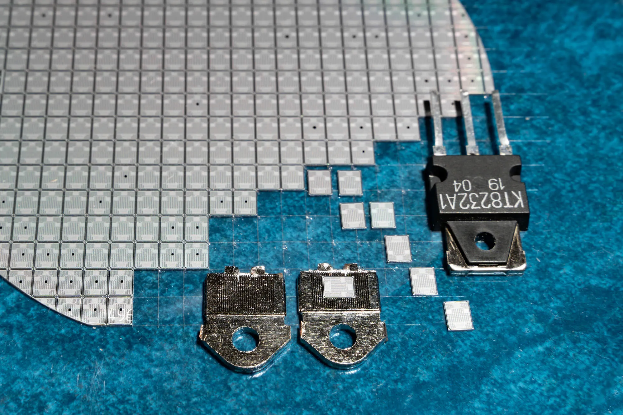
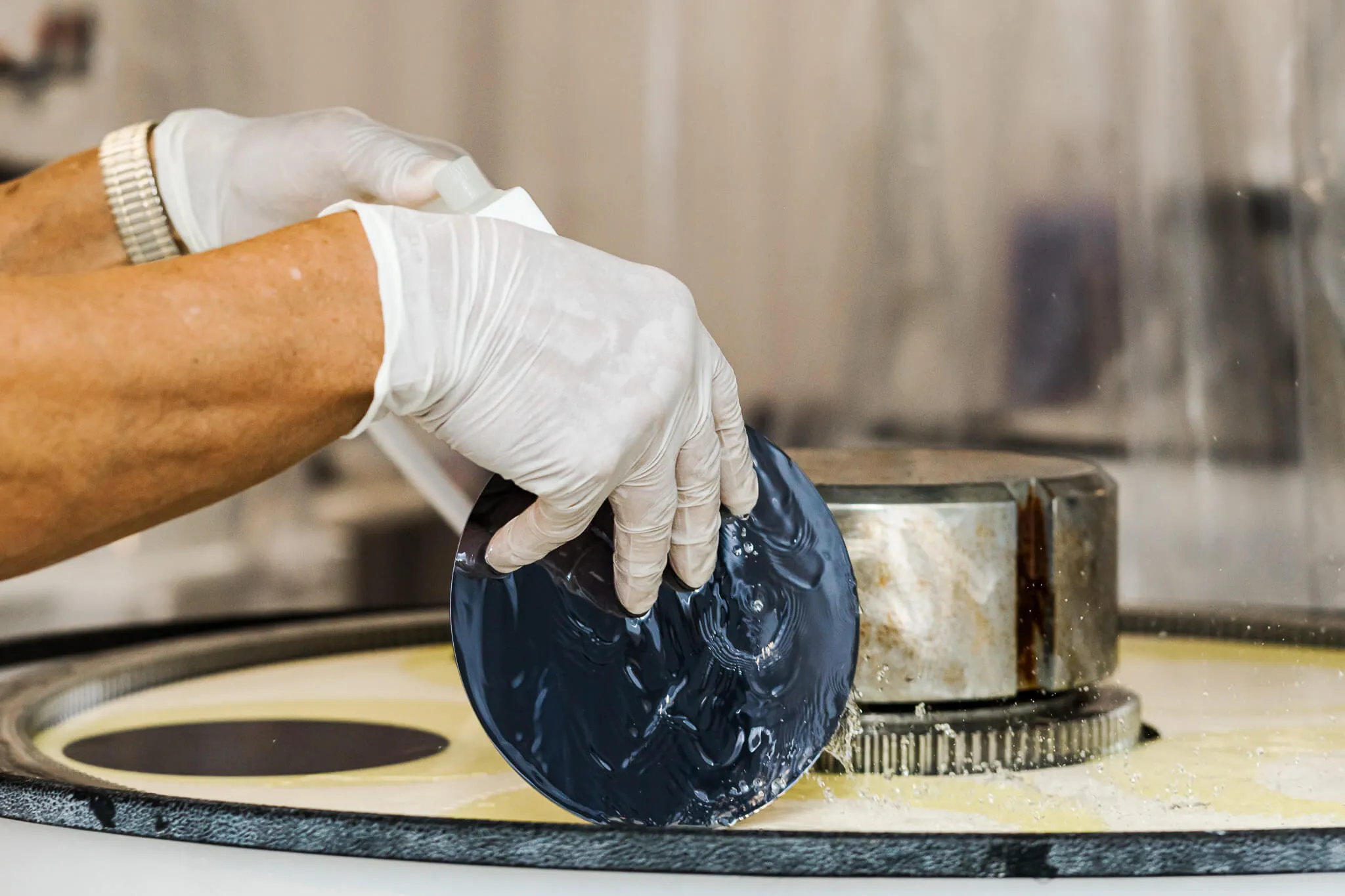
A wafer, also known as a semiconductor silicon wafer, is an essential part of the first steps in the production of chips because it is the "vessel" that converts integrated circuit designs into actual chips.
Germanium is another raw material for semiconductors that has many uses. It is frequently used in the production of solar cells, fiber optics, satellite image sensors, and military devices like night vision goggles.
The majority of germanium is generated either as a byproduct of processing zinc or from coal ash. China is the world's largest producer of germanium, accounting for 60% of production, and is expected to export 43.7 tons in 2022, according to the EU Critical Raw Materials Act (CRMA).
The remaining 40% of the Germanium in the world is produced in Finland, Russia, Canada, and the United States.
This semiconductor raw material, which can be found in trace amounts in zinc and bauxite ores, is used by producers to create gallium arsenide (GaAs). This is utilized in electronic chips and other applications like thermocouples, thermometers, nuclear medicine testing, and some medications.
Gallium metal, primarily produced in China and Japan, can be obtained through the processing of bauxite for the production of aluminum. Silicon semiconductor wafers cannot tolerate as high temperatures as gallium arsenide semiconductor wafers can, and they can function at higher frequencies.
Additionally, they have been shown to operate more smoothly than silicon semiconductor chips, particularly at high operating frequencies, which makes them useful for radar, LED lighting, satellite technology, and wireless communication devices.

This semiconductor material is widely used in the production of electronic devices due to its high reception, large emission current, direct bandgap, and low current density. In the field of optical telecommunications, indium phosphide is used in electronic devices such as laser diodes and integrated quantum optical circuits.
Moreover, indium phosphide has proven to be essential when creating integrated quantum optical circuits and laser beams. Its high sensitivity to radiation properties makes it a great option for optoelectronic device manufacturing, such as solar panel manufacturing.
Nevertheless, no raw material is perfect. One disadvantage of indium phosphide is its high cost and lack of a scalable production method, which makes it difficult to locate suppliers.
The material can be through the reaction between indium iodide and white phosphorus at high temperatures, by combining the pure elements at high temperatures and pressures, or by decomposing a mixture of phosphine and trialkyl indium compounds.
Doping is the process of adding impurities to silicon crystals to change their electrical properties in order to produce P-type and N-type semiconductors. P-type semiconductors have a lot of hollow holes, whereas N-type semiconductors have more electrons.
They can be combined to create a PN junction, which serves as the basis for different kinds of semiconductors.
All modern electronics are made possible by the precise electrical conductivity of silicon and other semiconductors, which is made possible by this essential manufacturing step. Two common materials used during doping impurities include:

Boron is a brittle metal that is essential to the production of semiconductor chips. By fortifying the bond between different materials, it increases their efficiency. Since it makes polymers more dielectric, boron is used in sealing pads, capacitors, and insulating layers on conductive wires.
Better signal transmission in optical fiber information systems is one of its benefits, which is made possible by the boron-doped fiber amplifier.
By serving as a dopant and occupying space in the crystal structure that was previously occupied by a silicon atom, phosphorus releases more electrons. While silicon's four valence electrons are replaced by its four, its fifth electron remains free to form no new bonds with other electrons.
It is commonly added by vapor deposition, gas diffusion, and direct injection into the silicon surface. The most widely used method for removing impurities from semiconductor raw materials used in integrated circuits is surface heating after phosphorus is deposited onto the silicon layer.
This process allows phosphorus to seep into the silicon. A lower temperature is then applied to stop the diffusion process.
The Global Semiconductor Raw Material Market Growth Report by Mordor Intelligence projects that the semiconductor material market will reach $70.30 billion in 2023 and will rise to $88.66 billion over the next five years.
The demand for raw materials is predicted to rise as semiconductor chip sizes continue to shrink. Additionally, the conflict between Russia and Ukraine has impacted the semiconductor supply chain.
These two countries are two essential raw material suppliers, so their dispute affected wafer manufacturers severely and drove up end-user costs. Additionally, it caused shortages and price increases for these materials that are necessary for the production of semiconductors and electronic components.

Semiconductor raw materials are essential to the completion of the semiconductor supply chain because they support each step of the chip-making process, from design and manufacture to packaging and final consumer electronics.
The future of the global semiconductor industry depends on comprehending its role and projecting the future production of raw materials. If you’re interested in learning more, reach out to Wafer World!