
A few years ago, Samsung’s Flip phone took the world by storm. Flexible optoelectronics applications are a new and exciting field for electronics, potentially changing how we interact with our devices. In this environment, we couldn’t help but wonder how much ultra flat wafers could influence this sector.
Ultra thin wafers are a fundamental component in thin film transistors (TFT), which are then integrated into screens. Here’s how that works.

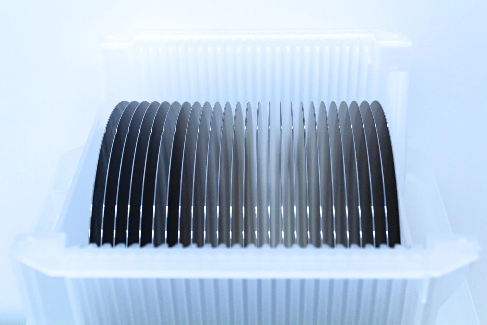
Ultra-flat wafers are achieved by combining chemical etching and mechanical lapping on bulk silicon wafers. They can be about 2 micrometers (μm) thick, making them ideal to produce thin-film transistors (TFTs). This lies in the wafer’s unique properties:
These thin-film transistors are then integrated into many display technologies.
Because of their flexibility and transparency, an ultra flat wafer’s potential can be exploited for:
Ultra-flat wafers' special qualities and uses are improving our daily lives by opening the door for more flexible and inventive electronics.
If you’re interested in learning more, reach out!


