
GaAs reclaim wafers’ unique properties make them ideal for electronic devices. Even after being reclaimed, the semiconductor’s utility and properties remain in top condition, offering effective results at lower costs. Despite all of this, silicon remains the go-to option for semiconductor manufacturers.
Maybe due to silicon’s availability as the second most abundant material on Earth or due to an already existing infrastructure, GaAs wafers haven’t become as widely spread as scientists anticipated. In this article, we’ll analyze the reasons why.
Silicon-based products have long ruled the semiconductor market. From computers and smartphones to solar panels, their dependability and affordability have made them a key component in our daily lives.
However, gallium arsenide (GaAs), a newcomer with a lot of potential, has entered the picture.
The combination of gallium and arsenic in semiconductors offers high electron mobility and direct bandgap properties that make it incredibly valuable in electronics, much more so than silicon.
When it comes to optoelectronic devices like solar cells and lasers, GaAs wafers are fantastic for high-frequency applications. They provide electronic devices with less noise, which greatly increases their dependability.
Moreover, GaAs have an advantage in aerospace applications where these characteristics are critical due to their intrinsic radiation resistance property and improved performance at elevated temperatures.
This has allowed GaAs wafers to overtake silicon in some industries despite silicon's lower cost and more established manufacturing base. Let’s explore that in more depth.
Silicon wafers have dominated the semiconductor industry. However, the potential of gallium arsenide, or GaAs, technology is becoming increasingly apparent.
Due to their dissimilar atomic configurations—arsenic has five valence electrons, whereas gallium has three—they combine to form a covalent bond that produces a direct band gap material with superior optoelectronic qualities.
GaAs's higher electron mobility than that of silicon makes it particularly effective in high-frequency applications like weak-signal amplification. It provides more flexibility by allowing electrons to move across various energy bands, in contrast to silicon, which confines electrons to particular energy levels or bands within its lattice structure.
Unlike silicon, GaAs also has low thermal conductivity. This can lead to significant thermal gradients across non-isothermal surfaces at sub-micron length scales.
These features necessitate accurate models that forecast temperature and heat generation, as well as a thorough understanding of heat generation within these devices for successful design applications.
Additionally, its unique valence structure gives it better dielectric qualities than silicon semiconductors. This versatility makes it essential for a wide range of electronic devices, such as light-emitting diodes (LEDs) and photovoltaic cells.
These alluring qualities have aroused curiosity among scientists worldwide, who are working tirelessly to maximize the potential of gallium arsenide by improving processing methods and expanding knowledge of this mysterious but intriguing material's properties.
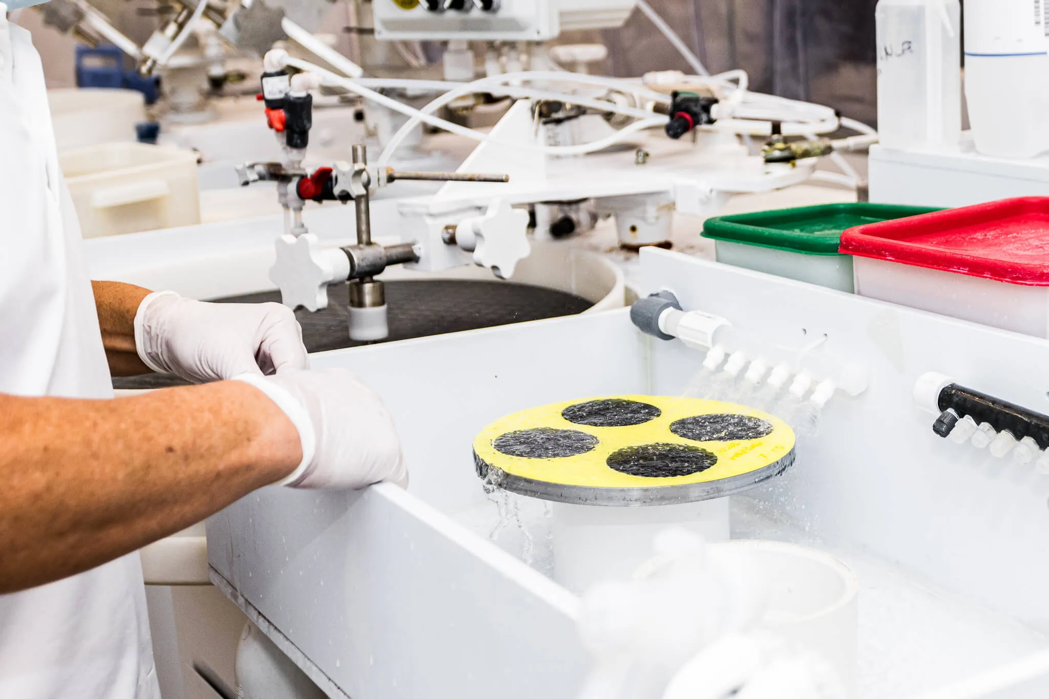
One of the challenges GaAs possess is their lower availability than silicon, but there are methods to reduce that difference. For instance, GaAs reclaiming helps reuse wafers and reduce material consumption and costs.

GaAs reclaimed wafers are wafers that undergo a restoration process to make them reusable, like a brand-new semiconductor.
During the reclaim process, wafers are stripped in automated wet immersion batch tanks and ground if they’re too thick. Lapping and edge rounding are also often performed on the reclaimed wafers.
After that, it is polished using a mix of chemical and mechanical polishing to get rid of any remaining slurry, undesirable particles, and metallic impurities. Finally, a thorough cleaning procedure is carried out.
Thanks to this meticulous process, GaAs wafers can be reused, lowering energy and electronic waste while returning them to their ideal state.
GaAs have attractive features, but they also present problems in terms of production processes when compared to standard silicon-based semiconductors.
Manufacturers need to employ sophisticated manufacturing methods, such as chemical vapor deposition or ion implantation, to create an epitaxial GaAs layer on a single-crystal GaAs substrate.
Additionally, while semi-insulating GaAs are faster and more responsive to frequency than their rival, Gallium Nitride (GaN), its performance is insignificant when considering thermal conductivity. Silicon outperforms these two materials by a large margin.
Additionally, even if reclaim processes increase the availability of GaAs, it will never reach the levels of silicon. Silicon is the second most abundant element in the Earth's crust, making up about 28% of its mass.
This transition—from trusted silicon technologies to unknown territories—is considered quite risky. Businesses are hesitant to give up their long-standing procedures centered around silicon semiconductors—especially considering that no proven aspects of contact reliability over time exist.
The change would mean significant costs and uncertainty about yield rates during the first stages of production ramp-up. Consequently, more establishments are drawn to this path and diligently investigate its possibilities.
This comes in a context where there’s a semiconductor shortage worldwide.
To meet the industry’s growing demands, silicon manufacturers have been working on increasing production and optimizing assembly lines, although this hasn’t been enough.
In this environment, where silicon prices may even increase, the shift towards GaAs wafers becomes an even riskier inversion.
Because of all of this, even though integrated circuit technologies that use GaAs have exciting growth potential, more research is necessary to address important concerns. Only then will manufacturers make the investments necessary to produce these wafers on a large scale, and widespread acceptance will become feasible.
Wafers are crucial elements in today’s technology. From cell phones to solar cells and even cars, most integrated circuits today depend on silicon wafers to work. And although there’s a shortage in relation to today’s demands, the abundance keeps producers free of worry.
Maybe for the same reasons, GaAs reclaimed wafers haven’t been such an attractive choice yet. Although these types of wafers offer unique properties, the market hasn’t properly embraced them yet, and they have only found a place in more specific industries. Still, there are opportunities for them to grow.
Here at Wafer World, we’re excited to see how much it will change in the future. If you’re interested in learning more about GaAs reclaimed wafers, reach out!


